“If you convert the electronic signals into light signals using separate chips, you lose a significant amount of signal quality. This also limits the speed of data transmission using light,” says ETH researcher, Ueli Koch.
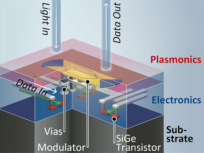
The integration was achieved by placing the electronic and photonic components on top of one another, and connecting them through vias.
This layering of the electronics and photonics shortens transmission paths and reduces losses in signal quality.
As demand for bandwidth pushes datacomms above 100 gbps transmission speeds, the ETH chip provides a way forwar“The rising demand will call for new solutions,” says Juerg Leuthold, ETH Professor of Photonics and Communications, “the key to this paradigm shift lies in combining electronic and photonic elements on a single chip.”For the past 20 years, the monolithic approach has failed because the features on photonic chips are much bigger than on electronic chips and the size of the photonic elements has made it impossible to combine them with CMOS.
“We’ve now overcome the size difference between photonics and electronics by replacing the photonics with plasmonics,” says Leuthold.As plasmonic IC features are smaller than electronic ones, it now becomes possible to manufacture much more compact, monolithic chips that incorporate both a photonic and an electronic layer.In order to then convert the electrical signals into optical signals, the photonic layer (seen in red in the graphic) contains a plasmonic intensity modulator. This is based on metal structures that channel the light in order to reach higher speeds.This is in addition to a speed increase in the electronic layer (seen in blue in the graphic). Through 4:1 multiplexing, four lower-speed input signals are bundled and amplified so that, together, they form a high-speed electrical signal.“This is then converted into a high-speed optical signal,” says Koch, “in this way, we were able to transmit data on a monolithic chip at a speed of over 100 gigabits per second for the first time.”The researchers combined plasmonics not only with classical CMOS electronics but also with BiCMOS technology.“We’re convinced,” says Leuthold, “that this solution can also pave the way for faster data transmission in optical communication networks of the future.
Source: This news is taken from www.electronicsweekly.com