But who is this small UK company that has been trusted to lead a consortium that includes semiconductor giant Infineon?The answer is: a fabless GaN power transistor maker built on technology invented at the University of Cambridge Engineering Department to address the fussy gate characteristics of GaN powertransistors.“We were founded in founded in 2016, got our first round of funding last year, and now we are leading a consortium,” CGD co-founder, CEO and inventor of the technology Giorgia Longobardi (left) told Electronics Weekly. “I am very proud of what my company has achieved.”
Some background
All GaN power transistors produced commercially so far are hemts (high electron mobility transistors).The issue with GaN hemts is that, in their basic form, they are inherently depletion-mode devices – they are naturally-on and conduct with no base drive, due to the metal gate’s Schottky contact and the strong two dimensional electron gas (2DEG) forming the channel at the AlGaN-GaN heterostructure.Very few power designers want depletion-mode behaviour, because it means the device becomes a short-circuit should the drive fail.This is a shame because GaN transistors are faster, are physically smaller, have less gate capacitance and less (zero) reverse recovery charge compared to similar silicon mosfets.To make them normally-off – enhancement-mode, like a silicon power mosfet – there are two commercial routes: cascode connection with a low-voltage silicon mosfet (Transphorm, Nexperia) or‘p-GaN gate’ (GaN Systems, Infineon). A third, ‘misfet’ (metal-insulator-semicondutor fet) approach is of research interest only at the moment.
Cascode
Cascode devices (Transphorm diag right) can be driven with standard chips designed to drive silicon power mosfets but, inside the package, a custom silicon mosfet crafted to match the GaN transistor’s switching characteristics has to be co-located within the package – adding to device complexity and on-resistance, as well as bringing in the inherent mosfet reverse diode with its annoying reverse-recovery current flow.
P-GaN gate
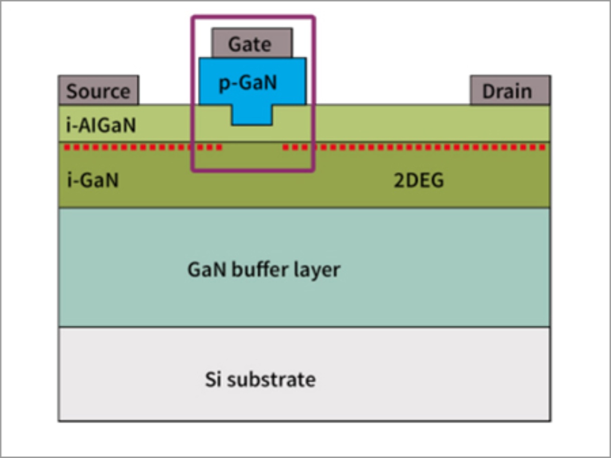
Its competitor, p-GaN gate (Infineon diag right), adds a charged layer to the GaN transistor between gate and channel which drives electrons out of the channel in the absence of gate bias, creating a normally-off device with no added on-resistance and no reverse-recovery issue. The drawback is that the gate is now fussy – easy to accidentally turn on as its threshold is only around a volt, and only tolerating around 6-7V before the gate (which is a diode) is heavily conducting into the channel.Special driver chips and circuits can and do address the 7V max value, and can manage the 1V threshold, but the gate remains vulnerable to accidental turn-on from high dv/dt and di/dt Miller transients from the drain – particularly high because GaN transistor drains can switch so much faster than those of silicon mosfets, and need to do so to achieve the product size reduction claimed for GaN technology.In some cases, gates need to be biased negatively to keep the GaN transistor off during turn-off – requiring an extra power rail and a negative-capable driver.
p-GaN gate with a twist
Cambridge GaN Device has a way to turn a 1V threshold 7V max gate into a >2V threshold gate that can withstand >15V, using only the standard GaN process technology of its chosen (un-named) foundry, said Longobardi.“We bring a technology that takes advantage of the foundry process,” she said. “It has a higher threshold voltage and wider allowable voltage for the gate. Customers like it because it is possible to drive it with a driver IC made for silicon mosfets and therefore makes GaN easy to use, which is Cambridge GaN Devices’ main goal.”Because of on-going intellectual property protection, Longobardi could not discuss details of the company’s technology, but did reveal that it takes an integrated circuit approach, building extra GaN devices on the substrate around the main GaN power transistor, which CGD also designed.
The GaN-on-silicon process used is the same that would be used to make a single GaN power transistor.“Our solution is at layout level rather than process level,” she said. “We don’t change metal types or anything, we just use the fab’s recipe.”This approach puts the gate characteristic modification circuit right next to the transistor gate, reducing parasitic inductance that might scupper external schemes.So what business model is being built around the technology?“We are going to become a supplier of GaN transistors,” said Longobardi. “We have ambition to be the number one supplier of GaN transistors.” Products will be available “very soon”.The basic version will be three-terminal, or four-terminal with a Kelvin source connection.According to Longobardi, this will include all that is needed to modify the gate voltages without needing extra substrate area or adding cost.Beyond that, more intelligence can be added. “It depends on how much smartness you include. Different applications require different features. If you add all that we have, then it will need some additional area,” she said.
Source: this news is taken from www.electronicsweekly.com