They are based on the company’s SenSWIR technology, with photodiodes formed in an indium gallium arsenide (InGaAs) layer, Cu-Cu connected to a silicon readout circuit – allowing broadband sensitivity from 0.4μm to 1.7μm (blue to IR).
Copper-copper bonding is important, according to Sony, because this allows a closer pixel spacing that is available using conventional conventional bump connections.
Bruises in apples, not visible to the eye, exposed by infra-red imagingIn addition, it allows “Sony’s original technology to make the top InP layer, which absorbs visible light, thinner, making it possible to transmit light to the InGaAs layer underneath, delivering high quantum efficiency even in the visible range” – allowing one camera to be used instead of separate visible and SWIR cameras.
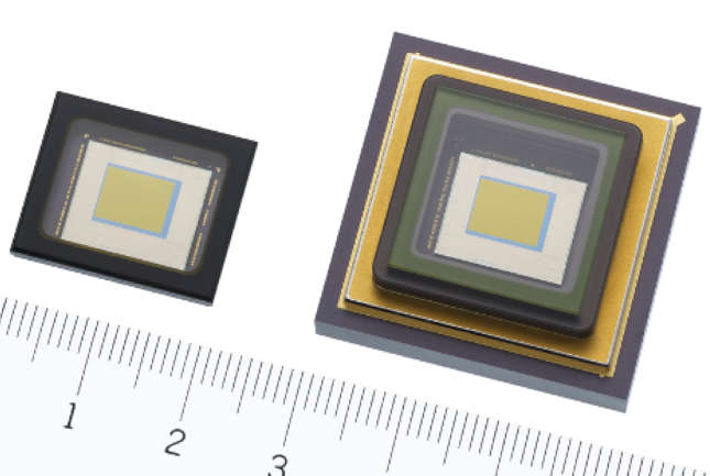
The parts are:
IMX990 – 1,296 x 1,032 1.34Mpixel SXGA with 8.2 mm diagonal (‘1/2-type’)
Frame rate, full pixel: 130frame/s (8bit), 120frame/s (10bit) or 70frame/s (12bit)IMX991 – 656 x 520 340kpixel VGA with 4.1 mm diagonal (‘1/4-type’)
Frame rate, full pixel: 250frame/s (8bit), 240frame/s (10bit) or 130frame/s (12bit)
Common specs are:
5μm x 5μm unit cell
Power: 2.2V, 1.2V (pixel); 3.3V, 2.2V (analogue); 1.2V (digital); 1.8V (interface)
global shutter, digital thermometer, ROI functions
SLVS output (2/4ch switching)
30 x 30 ceramic PGA with built-in thermoelectric cooling
20 x 16.8mm ceramic LGA
Source: This news is taken from www.electronicsweekly.com