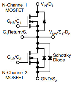
The mosfets are optimised for their respective tasks in a buck converter (see table and diagram). One has a maximum on-resistance of 4.5mΩ at 10V (7.0mΩ at 4.5V) and typically 6.9nC gate charge, and the other is 1.84mΩ at 10V (2.57mΩ at 4.5V) and typically 9.4nC.Current rating is 20-30A, or more, depending on temperature and heatsinking – see data sheet.“The device provides designers with a space-saving solution for point-of-load conversion, power supplies, and synchronous buck and dc-dc converters in graphic and accelerator cards, computers, servers, and telecom and RF networking equipment,” according to Vishay.“The dual mosfet features a unique pin configuration and construction that delivers up to 11 % higher output current per current phase than competing products in the same footprint area, in addition to higher efficiency for output current above 20A.”
Source: This news is taken from www.electronicsweekly.com